HTPB (Hydroxyl-Terminated Polybutadiene), as a high-performance elastomer, offers
unique advantages in potting applications for electronic materials, particularly in
scenarios requiring flexibility, weather resistance, and electrical insulation.
Below is a summary of key points regarding the use of HTPB for electronic potting:
**1. Characteristics and Advantages of HTPB for Potting**
1. - Flexibility and Impact Resistance: Upon curing, HTPB forms an elastomer that absorbs mechanical stress, protecting sensitive electronic components (e.g., sensors, circuit boards) from vibration or thermal expansion.
2. -Electrical Insulation: High volume resistivity (>10¹⁴ Ω·cm), making it suitable for high-voltage insulation or high-frequency signal transmission.
3.- Chemical and Weather Resistance: Resistant to acids, alkalis, and UV radiation, ideal for outdoor electronic devices (e.g., PV junction boxes, automotive electronics).
4.- Low Curing Shrinkage: Minimizes internal stress post-potting, preventing component deformation or cracking.
5.- Moisture and Dust Resistance: Provides effective protection against environmental contaminants.
**2. Potting Material Formulation Design**
- Curing System Selection:
- Isocyanates (e.g., TDI, IPDI): Forms polyurethane networks; NCO/OH ratio (typically 1.05–1.1:1) must be controlled to balance hardness and elasticity.
- Peroxide Curing: Suitable for high-temperature applications but may reduce flexibility.
- Filler Additives:
- Thermal Conductive Fillers: Boron nitride (insulating and thermally conductive), alumina (cost-effective).
- Flame Retardants: Aluminum hydroxide, phosphorus-based flame retardants to meet UL94 V-0 standards.
- Plasticizers: e.g., DOA (Dioctyl Adipate) to further reduce modulus, though migration risks must be evaluated.
**3. Typical Applications**
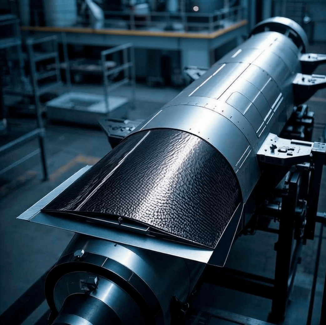
1. Military/Aerospace Electronics: Potting for missile circuits, radar components, leveraging HTPB’s broad temperature range (-50°C to 80°C).
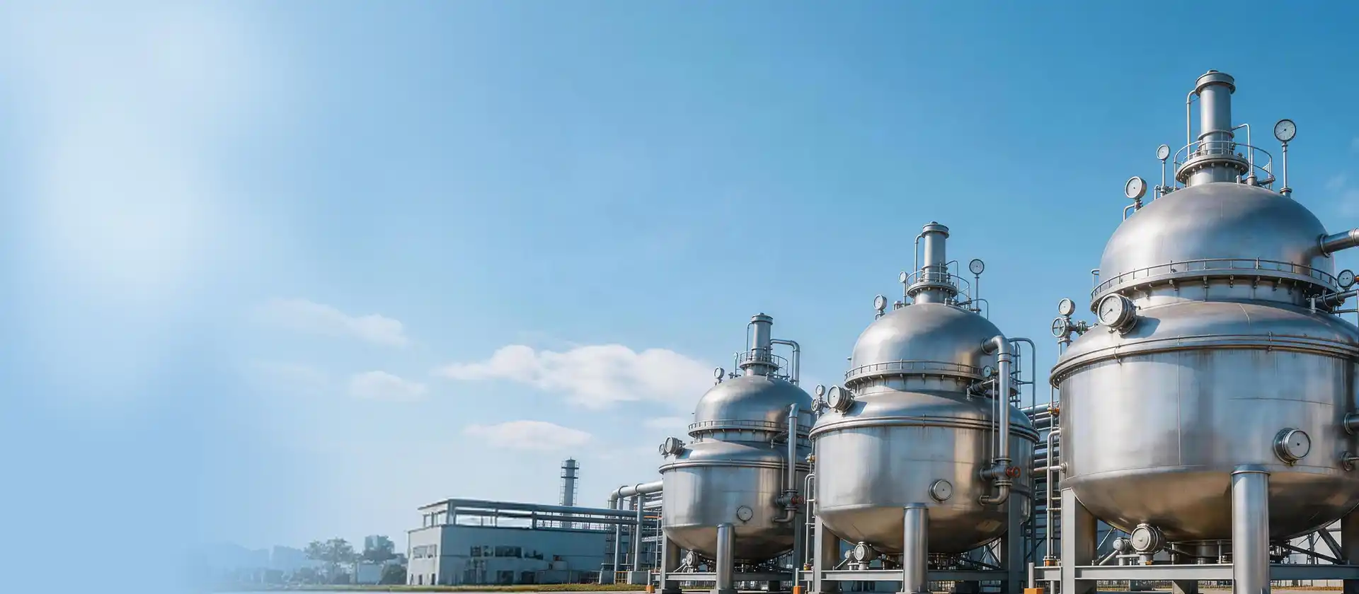
2. New Energy Sector: Lithium battery pack encapsulation, charging module protection, balancing insulation and shock absorption.
3. Underwater Equipment: Submarine cable joint potting, resistant to saltwater corrosion and waterproof.
4. Printed circuit boards ( PCBs)
5. Telecommunications and Network Infrastructure
6. Renewable Energy and Power Electronics
7. Marine Electronics
8. High-Durability Consumer Electronics
**4. Process Considerations**
- Bubble Removal: Vacuum degassing (-0.095 MPa, 10–20 minutes) to prevent air pockets after curing.
- Curing Conditions: Room-temperature curing (24–48 hours); heating (60–80°C) reduces curing time to 4–8 hours.
- Pretreatment Adhesi: Perawatan plasma atau primer diperlukan untuk substrat non-polar (misalnya PE) untuk meningkatkan ikatan.
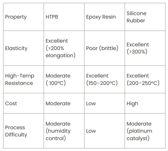
**5. Perbandingan dengan Bahan Pot Lainnya**
**6. Strategi Peningkatan**
- Modifikasi Nano: Memasukkan nano-SiO₂ untuk meningkatkan kekuatan mekanik (misalnya, kekuatan tarik meningkat dari 5 MPa menjadi 8 MPa).
- Sistem Campuran: Ko-polimerisasi dengan epoksi (misalnya, jaringan interpenetrasi EP/HTPB) untuk menyeimbangkan kekakuan dan ketangguhan.
Bahan pot HTPB sangat cocok untuk perlindungan elektronik di lingkungan yang dinamis, dan formulasinya harus dioptimalkan berdasarkan persyaratan kinerja spesifik.
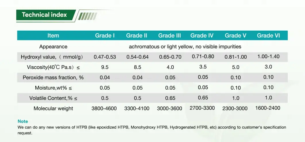
Perusahaan kami menawarkan HTPB dalam berbagai tingkatan dan menyediakan produksi yang disesuaikan berdasarkan spesifikasi klien yang diperlukan.
 English
 English
  Spanish
  Russian
  Arabic
  French
  German
  Portuguese
  Turkish
  Dutch
Dutch  Polish
  Korean
  Vietnamese
  Indonesian
 01. Apr, 2026